‘The making of a microchip is a very delicate process – even a single dust particle smaller than a virus can destroy an entire wafer worth millions of dollars’. It’s like building a skyscraper on a grain of sand – one mistake and the entire building will collapse.
“A state-of-the-art chip can contain over 100 billion transistors” – This is why the semiconductor manufacturing process is one of the most challenging and high-precision work on this planet, requiring Clean room manufacturing. (Source – Apple)
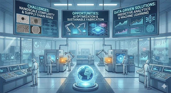
And this is where modern challenges collide with modern solutions.
Excited to discover the challenges and solutions? Keep reading this post to navigate complexities, opportunities and data-driven solutions in the semiconductor manufacturing industry.
Understanding the Semiconductor Manufacturing Process
Manufacturing of the chip starts with pure silicon – a wafer. From here, dozens – and sometimes hundreds of steps follow – lithography, etching, doping, packaging and more.
Imagine printing a nearly invisible city on a cheese cake and that too layer by layer – way too complex, right? This is how chip making works. Each layer has to be aligned within nanometers of space – any misplacement or variation can destroy it.
As the node shrinks – say to 4nm or below – the accuracy grows exponentially. Which means more steps, more tasks and more process complexity.
Major Semiconductor Process Challenges Today
The production of semiconductors is not just expensive but complex, too. Let’s explore the major challenges today:
Resource Demand – Building a fab costs around $15-$20 billion when equipped fully. It requires plenty of cost to get started.
Technical Barriers – Lithography is used in nodes – process of printing circuits on silicon. The machines used in this cost millions of dollars and any instability can degrade yield or stop production.
Operational Uncertainty – As the equipment is specialized – only a few suppliers control specialized gases, optics and others, increasing operational uncertainty.
Industry insights According to the 2025 white paper by Fractilia, “random patterning variations” in lithography at the latest process nodes are now causing hundreds of millions of dollars in yield loss per fab and represent the single largest barrier to achieving reliable high-volume manufacturing at cutting-edge nodes.
Data-Driven Process Control & Yield Optimization
With the blade thin margins between success and wafer scrap, modern fabs are relying more on data. It’s process is like a high-stakes orchestra – thousands of instruments (machines) tuned in real time.
It has sensors everywhere to monitor temperature, pressure and more, feeding data to centralized sensors for real-time control. AI and ML predict maintenance needs – effectively acts like a “chip doctor”.
This results in fewer defects, less waste and quicker processes – often a difference between the profit and loss.
Supply Chain & Equipment Ecosystem: Building Resilient Manufacturing
Chipmaking depends on a fragile supply chain where even a single missing gas or tool can halt production:
Relying on a few suppliers creates big risks.
Sourcing from multiple regions adds stability.
Strong partnership with tool producers improves uptime.
Sustainability, Efficiency & Environmental Impact in Chip Fabrication
Semiconductors’ huge energy and water use make sustainability an urgent concern.
Sustainability Fact A modern fab can consume 10-20 million gallons of ultrapure water per day.
But here is a progress – leading manufacturers are investing in water recycling systems, energy-efficient cleanrooms and alternative low-emission chemicals.
Adopting sustainable options doesn’t just reduce environmental harms – but also lowers operational costs.
Preparing for the Future: Strategies for Semiconductor Manufacturers
The future of the semiconductor manufacturing industry belongs to the companies that stay flexible, adapt to smart automation and build stronger supply chain partnerships. Rather than chasing complexities, winners will focus on tightening operations, adopting AI driven workflows and reducing their dependency on fragile global networks.
Success is now more dependent on doing fewer things – but doing them exceptionally well.
Protecting IP, modernizing production lines, building reliable supplier ecosystems and training teams to adapt quickly are the best practices to follow. As the industry faces a rapid shift in demands and regulation, manufacturers work with future planning and operate with clarity while staying competitive.
The upcoming path is simple: streamlined, automated, collaborative and evolved faster than the market.
FAQs
Ans: Chip manufacturing is extremely complex because modern features are smaller than viruses, meaning even tiny variations can damage or ruin an entire wafer.
Ans: Most yield losses occur due to patterning variability, equipment failures, and microscopic material defects that become especially critical at sub-5nm process nodes.
Ans: Semiconductor fabrication plants consume large amounts of water and energy, so companies are increasingly adopting water recycling systems, renewable energy sources, and greener chemical processes to improve sustainability.